Prototype number zero mainboard and no magic smoke 2007-06-09
After about two weeks of almost constant work in the evenings and late into the night, I've managed to produce the first prototype mainboard and a number of sensor module prototypes will be completed today. The electronics required aren't particularly advanced but I've had to greatly improve and develop a number of my design and fabrication skills.
The goal of the prototype 0 mainboard is to be able to capture and record the inputs from a number of different sensor modules and store the data for future processing. The main components for the mainboard are a CPU (Analog Devices EVAL-ADUC7020MK Minikit), power supply regulation (LM2576, LM1117), host interaction (MAX232), SD/MMC card adapter, connection points for digital and analog inputs, and a Dual UART (SC16IS752) for interfacing with serial sensor modules. I also added loads of prototype pads which should allow me correct any mistakes or add missing features.
I used the open source tools gschem and pcb to design and layout the schematic and circuit board.


I took a number of photos of the steps I did when going from the circuit board layout to the finished board. I used the photo-resist process to produced a double sided board, I didn't plate the holes but I soldered pins on both sides of the board to join the layers. Notes (almost tutorial) for each photo are from left to right, top to bottom.
- I used a laser printer to print out the appropriate mirrored layers (solder, component) on to clear film (acetate) sheets.
- I lined up the holes and created an envelope which will contain the board.
- I used pre-coated photo-resist copper clad boards, I cut the board to side and then clear fully remove the film.
- I placed the board inside the envelope, and taped the corners which I had cut at an angle to securely film while being exposed.
- I have a UV box and placed and exposed the board on each side for 4 minutes.
- It is possible to see the slight change in color caused by the exposure.
- Clear full pour the developer onto the board in a tray. Note: These chemicals are hazardous and damaging so wear rubber gloves and eye protection, and preform these steps in a shed or work room.
- Gently rock the tray, you should see the board appear, turn the board so that both sides are developed.
- When the board is developed remove it from the developer and rinse it thoroughly in water. Look for any imperfections, the photo-resist I used is green in color so the imperfections should clearly standout. If there are any area which need a touch up use a suitable (Red Staedtler Lumocolor 313) permanent pen to make the corrections.
- I then placed the board inside another clean tray which was inside a larger tray containing hot war, like a bain-marie or double boiler. I then carefully poured in the etchant (Ferric Chloride, FeCL3).
- Gently rock the tray, after about five minutes depending on the side of the board temperature, and concentration of the etchent you should start to see the copper dissolve away.
- Once the etching has finish rinse the board thoroughly in water.
- The photo-resist lay needs to be remove, by exposing the board in the UV box placing back in the developer or rubbing with a polishing block.
- Drill the many holes, you'll get the best results using a drill-press or desk-mounted drill. Polish and clean the board before soldering.
- I used a combination of solder paste and wire solder depending on the type of component.
- The top side of the board.
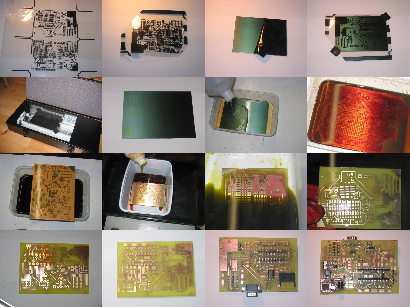
Here is the finished board.


The design of the board isn't perfect. ;) Two problems I've noticed so far is that I never added any LED indicators to show if the power is working etc., and I never linked the IRQ pin on the Dual UART to the CPU.
I was very cautious when first powering up the board, and used a very basic current limiter circuit, so no magic smoke was released. And when I plugged the serial cable into my computer and reset the CPU I was greeted with the fabulous words 'Hello World!'.